The group has its research focus on optical and electrical properties of emerging low-dimensional nanomaterials, such as semiconductor nanocrystals, metal nanostructures, two-dimensional layered perovskites, and on hybrid systems that benefit from advantageous properties of those materials. Low-dimensional semiconductor nanomaterials can be excellent light emitters or absorbers, and the optical properties like for example the light emission wavelength, direction and polarization can be controlled via their architecture, size, shape and composition.
This makes them very interesting as active material in light-emitting, lasing, or photovoltaic devices, and we are exploring novel approaches for proof of principle prototypes. On the other hand, metal nanostructures are very good conductors and can strongly interact with light in the visible and infrared spectral regions due to the presence of free electrons that can perform plasmon oscillations, which opened the field of nanoplasmonics.
Recently, two-dimensional layered perovskites have has attracted great interest since they combine organic and inorganic layers, and thereby provide a vast range of opportunities to tailor their properties by designing their architecture and composition. We aim at combining the favorable properties of these materials in order to investigate complex optoelectronic systems and to pave the way for novel architectures for components in photodetectors, optical communication, photovoltaics, plasmonics, and nanoscale electronics.
- Our work on heterostructures in 2D layered perovskites has been published in Advanced Materials.
- The recent results of our studies on the vibrational properties in 2D perovskites and the impact of electron-phonon coupling on the light emission has been published in Nano Letters and Accounts of Chemical Research, where it was featured on the back cover.
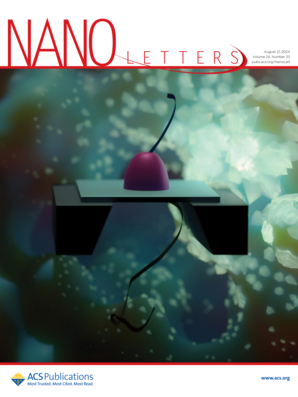
- We succeeded to fabricate 3D nanopores with different shapes made from metal oxides with high robustness and nanoscale control of their aperture (published in Nano Letters and featured on a supplementary cover).
- Soon we will have new openings for PhD and postdoc positions, please contact Roman Krahne if you are interested.
- Our work that shows how the efficiency of light-emitting diodes could be enhanced by the integration of layered metamaterials has been published in Advanced Optical Materials.
- Congratulations to Alexander Schleusener for winning the MSCA European Fellowship with his project TOGETHER!
- Our work on the directionality of the phonon bands in layered perovskites, and their relation to the broad band emission is published in Small.
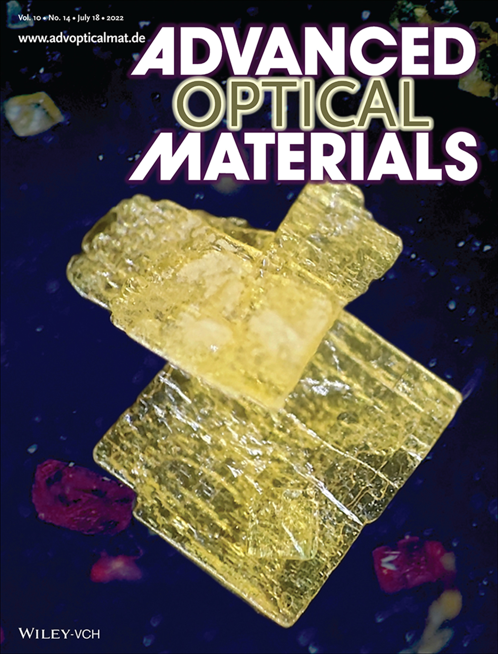
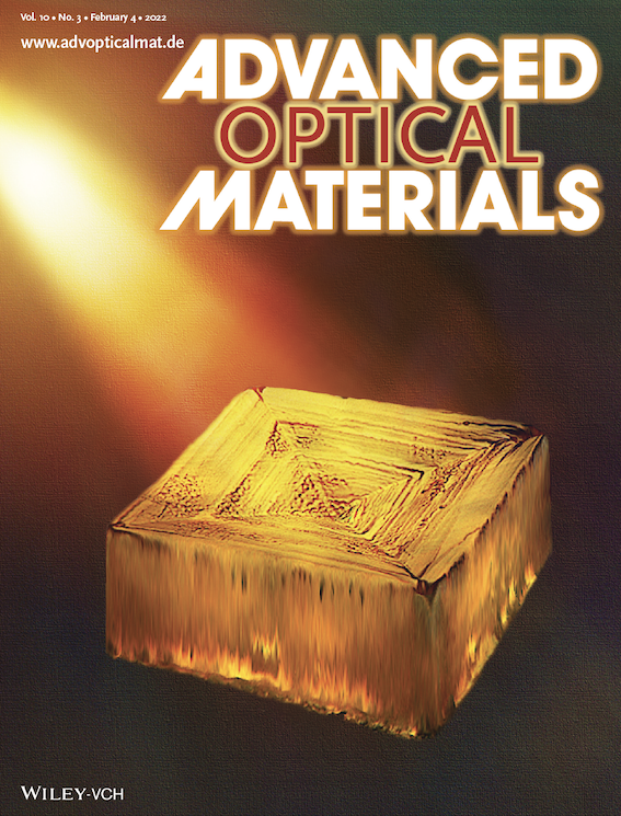
- Our paper that reports on the optical and photoconductive properties of CsPbBr3 microcrystals appeared on the inside cover of Advanced Optical Materials.
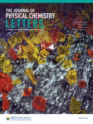
Layered Metal-Halide Perovskites: These emergent materials consist of organic/inorganic bilayer architectures and demonstrate many interesting properties such as strong quantum confinement and high exciton binding energies. Based on the fabrication route that we developed to obtain warm white light to blue light emission [B. Dhanabalan et al., Adv. Mater. 2021, 33, 2008004], [Dhanabalan et al., Nanoscale 2019, 11, 8334], we investigated the formation of lateral heterostructures by solution based chemistry [A. Schleusener et al., Adv. Mater. 2024, 36, 2402924]. We are interested in the impact of the organic cation on the the optical and vibrational properties and revealed distinct directionality of the vibrational modes [Dhanabalan et al., ACS Nano 2020, 14, 4689] that also has significant repercussions on their light emission. [Krahne et al., Nano Lett. 2024, 24, 11124], [Krahne et al., Acc. Chem. Res. 2024, 57,2476]. Towards lead-free systems we are interested also in AgBi double perovskites where we investigate their structural and optical properties, revealing phase transitions that involve both organic and inorganic layers, [Martìn-Garçia et al., J. Phys. Chem. Lett. 2020], and directionality of lattice vibrations. [Martín-García et al., Adv. Opt. Mater. 2022, 10, 2270056]
Metamaterials: We develop layered Metal/Insulator/Metal structures as photonic and plasmonic cavities, and demonstrate that their resonances correspond to Epsilon-near-zero (ENZ) modes. Such cavities be used for light emission enhancement of semiconductor nanocrystals by the Purcell effect [V. Caligiuri et al., ACS Photonics 2018, 5 , 2287–2294], to modulate the emission properties of dyes inside the cavity [V. Caligiuri et al., Adv. Opt. Mater. 2019, 8, 1901215], as ultrafast switches [J. Kuttruff et al., Communication Physics 2020, 3, 114], and for strong light matter interaction [A. Patra et al., Nano Lett. 23, 1489-1495 (2023)]; [A. Patra et al., Adv. Opt. Mater. 2021, 9, 2101076]. Deeper physical insights into such ENZ modes by a semiclassical treatment of the optical resonances of this material system are reported [V. Caligiuri et al., Nano Letters 2019, 19, 3151-3160]. Coupled Cavity systems with multiple resonances and ENZ bands are discussed in [V. Caligiuri et al., Nanophotonics 2019] and [V. Caligiuri et al., Adv. Photon. Res. 2021, 2, 2100053].
Solid state nanopores: Within our European projects on DNA data storage (DNA-FAIRYLIGHTS) and single molecule detection (DYNAMO) we are developing solid state nanopores with controlled shape, aperture and different material composition, [Lanzavecchia et al., Adv. Opt. Mater. 2023, 11,2300786], such as polymers and metal oxides, and we investigate their functionality in DNA detection, current rectification and as memristors. [Lanzavecchia et al., 2024, Nano Lett. 24, 10098]
We have labs for optical and electrical sample characterization, as well as access to the IIT clean room, Materials Characterization, Nanochemistry, and Electron Microscopy facilities. In our ultrafast spectroscopy lab we have femtosecond pulsed laser sources (Coherent Legend Elite), time-resolved photoluminescence (PL) spectroscopy (Edinburgh FLS920) and custom made setups for measuring amplified spontaneous emission and micro-PL. For photoconductive characterization we use micromanipulator probe stations in ambient (Karl Suss) and cryogenic (Janis Research) environment that can be coupled to various light sources and lasers spanning the spectral range from UV/VIS to NIR for photoelectrical characterization. Piezo-controlled mibots (Imina) reaching nanometer control can be used for probe contacts with optical and electron microscopes.
- Coordinator of the Horizon Europe MSCA Scientific Exchange project DELIGHT (2024-2027)
- Coordinator of the Horizon Europe MSCA Doctoral Network DYNAMO (2022-2026)
- Coordinator of the H2020-FET project DNA-FAIRYLIGHTS (2021-2025)
- Prof. Pingheng Tan, Chinese Academy of Sciences, Institute of Semiconductors
- Prof. Davide Comoretto, University of Genoa
- Dr. Alexander Weber-Bargioni, Lawrence Berkeley National Lab, California, USA
- Prof. P. James Schuck, Columbia University, New York, USA
- Dr. Cinzia Giannini, IC-CNR, Bari, Italy
- Prof. Iwan Moreels, University of Ghent, Belgium
- Prof. Antonio De Luca, University of Calabria, Italy.
- Prof. Sandrine Ithurria, École Supérieure de Physique et de Chimie Industrielles, Paris France.
- Prof. Antonio De Luca, University of Calabria, Italy.
- Prof. Sandrine Ithurria, École Supérieure de Physique et de Chimie Industrielles, Paris France.
Roman Krahne was appointed Honorary Professor at the Institute of Semiconductors, Chinese Academy of Sciences.
Optoelectronics
